Hardware Interface
This section delves into the hardware interface of the SidecarT board, specifically the way the board and the code in the RP2040 handle the mismatch of the size of the buses between the RP2040 and the Atari ST cartridge port.
Table of contents
- The Atari ST Cartridge Port
- Exploring the GPIOs of the Raspberry Pi Pico W
- Reading the Atari ST Cartridge Address bus and Writing on the Data bus
- Building pure time multiplexing on a multiplexed bus with the RP2040
- A1 to A15 address bus without ROMx signals
- A1 to A15 address bus with ROMx signals control
- How to orchestrate the access to the Atari ST cartridge address and data buses
The Atari ST Cartridge Port
Overview
The Atari ST, unveiled in the mid-1980s, boasted a cartridge port that, paradoxically, was not immensely popular, defying the widespread trend of cartridge utilization in computers and gaming consoles of that period.
The cartridge port of the Atari ST served as a direct extension of the system’s bus, reflecting the era’s prevailing hardware technology and design ideologies.
The port adopted a double-row 40-pin configuration, engineered to gain direct access to the system’s bus. This allowed external cartridges to interface seamlessly with the main system without the necessity for intricate adapters or converters.
Typical of many computers from its epoch, the Atari ST was grounded in TTL (Transistor-Transistor Logic) technology, defining logical levels (high or low) through standard TTL voltage levels. Furthermore, the cartridge port offered a +5V power pin to energize the cartridges, aligning with the TTL logic levels utilized in the Atari ST. Ground pins were also furnished to form the electrical circuit and ascertain stable operation.
Despite the Atari ST’s CPU clock functioning at 8MHz, its system clock operated at a mere 2MHz—quadruple the speed of the CPU clock. During each system clock cycle, the CPU could delegate a memory address on the bus to read, obtaining a response on the data bus from the device in the cartridge port within approximately 500ns. More can be learned from this article.
Address, Data, & Control Lines
The cartridge port was designed with a limited number of 68000 control lines to simplify cartridge construction, thereby enabling developers to forge various hardware expansions without confronting the multifaceted intricacies of interfacing with the 68000’s control lines. The Atari ST’s designers deliberately engineered the cartridge port to be read-only. This decision was due to a desire to simplify control lines or potentially due to financial constraints. Although this read-only characteristic limited certain solutions dependent on the cartridge, it inadvertently catalyzed the development of ingenious alternatives.
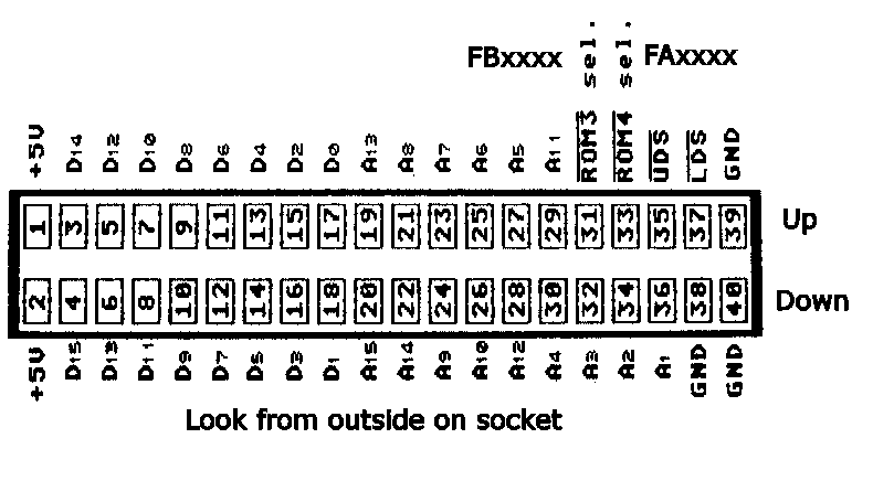
Serving as an extension of its primary system bus, the Atari ST’s cartridge port utilized 24 address lines (A0-A23), enabling it to address up to 16MB (2^24 bytes) of memory, which was limited to 4MB due to some address space being allocated to ROMs and peripherals. A mere 17 address lines (A0=!UDS, A1-A15, A16=!ROM4) were routed to the cartridge port, used to access the memory range from FA0000 to FBFFFF, thereby addressing a substantial 128 Kbytes of ROM memory effectively.
The Atari ST incorporated a 16-bit data bus, correlating with data lines D0-D15. This allowed a 16-bit word to be transmitted in a single bus cycle. The UDS and LDS lines addressed either the upper or lower 8 bits of this 16-bit word, thus permitting byte-level access. The data lines were read-only.
In addition to the address and data lines, several control lines were crucial for SELECTing the ROM and determining which parts of the data lines to read. These encompassed the ROM SELECT lines ROM3 and ROM4, as well as UDS and LDS, which were integral for upper and lower byte SELECTion.
Exploring the GPIOs of the Raspberry Pi Pico W
Overview
The Raspberry Pi Pico and Pico W, endowed with a versatile array of 40 pins, facilitate connections to various electronic components. Among these, 26 programmable General Purpose Input/Output (GPIO) stand out, offering a gateway for enthusiasts and developers to interface with peripherals, or to foster communication with other microcontroller/microprocessor boards.
The Raspberry Pi Pico extends support for the subsequent peripheral interfaces on its pinout:
- 2x UART
- 2x I2C
- 2x SPI
- 16x PWM channels
- 4x ADC pins
The RP2040 GPIOs can play different roles depending on the configuration given. For SidecarT, we will use as pure GPIOs pins. The RP2040 GPIOs can be configured as inputs or outputs, and the direction can be changed dynamically. The RP2040 GPIOs can also be configured to have a pull-up or pull-down resistor, and the resistor can be enabled or disabled dynamically.
Of the remaining 14 pins, the Raspberry Pi Pico possesses numerous power pins, including 3V3 (OUT), VSYS, and VBUS, which are demarcated as red on the pinout diagrams. Moreover, several ground pins are presented, marked in black on the pinout diagrams, while the remaining pins are designated for internal GPIOs and ground connections.

The SidecarT GPIOs
In our configuration, the GPIOs are attributed to the following functions:
- GP0-1: UART0 TX/RX - output
- GP2-4: SPI0 CLK/MOSI/MISO - output
- GP5:
SELECTbutton - input - GP6-21:
!UDS=A0, A1-A15 - input / D0-D15 - output - GP22:
!ROM3- input - GP26:
!ROM4- input - GP27:
!READ- output - GP28:
!WRITE- output
There are three pins that are very important for developers but not for users not willing to develop their own software. These pins are the SWD pins, which are used to program the RP2040. The SWD pins are not used by the SidecarT software, but they are used by the Raspberry Pi Pico SDK to program the RP2040. Please see the section on Software Development for more information.
As a prudent guideline, altering the direction of the GPIOs is typically discouraged unless executed with impeccable timing. The modulated directional change of GP6 to GP21 every 250ms—implemented to read the address bus and write the data bus—emerges as an optimal solution, adeptly navigating the discrepancy in bus sizes between the RP2040 and the Atari ST cartridge port, as will be explored in the ensuing section.
Reading the Atari ST Cartridge Address bus and Writing on the Data bus
The Atari ST runs at 8MHz, so each clock cycle is 125ns. But the system clock cycle is 4 times the CPU clock cycle, so the CPU clock cycle is 500ns. This is the lapse of time a ROM cartridge has to read the address bus and write the data bus.
The signals governing the access to the address and data bus of the cartridge are !ROM3 and !ROM4 (they are inverted signals) and specifically when !ROM4 or !ROM3 signals are low. During this time, the cartridge can have access to the Motorola 68000 address bus and the write data bus. It is guaranteed that there will not be any contention conflict with the Atari ST memory bus.
The !LDS and !UDS signals are used to SELECT the upper or lower byte of the data bus. The !LDS signal is active when the lower and the !UDS signal is active when the upper byte of the data bus is SELECTed. !LDS and !UDS are directly connected to the Motorola 68000 signals, so it’s not worth to use them to control the RP2040, unless you want to use them jointly with the !ROM3 and !ROM4 signals. So from the bus synchronization perspective, let’s forget about the !LDS and !UDS signals from now on.
Hence, we have to focus on !ROM3 and !ROM4. So this is the algorithm we have to implement to emulate a ROM device:
- Wait until the
!ROM4or!ROM3signals are low (ACTIVE). We have to assume that this change of state won’t take longer than 125 nanoseconds (1 Atari ST clock cycle). - Read the address bus and wait until the address information is stable. This should not take more than 1 Atari ST clock cycles (125ns) and the remaining time not consumed in step 1.
- Send the information to the data bus and wait until the data is stable. This should take 1 Atari ST clock cycles (125ns) plus the remaining time not consumed in step 1 and 2.
- Wait until the
!ROM4or!ROM3signals are high (INACTIVE) again and repeat the process (125ns) or the reamining time until the next 500ns clock cycle starts.

This diagram represents the ideal behaviour of a read data access in the Atari ST cartridge. The red columns represents the address bus access and the blue columns represents the data bus access. An Atari ST program requests to the &FA0001, &FA0003, &FA0001, &FA8007 addresses to return from the memory a word value (in this example it returns the value of the address). Since the example is simply an example of the ideal usage, the address data stays in the address bus even when the data bus is populated with the result, until the !ROM4 is deactivated again. As we will see, this is not the case in the SidecarT implementation.
So the !ROM4 (it could be !ROM3 as well) are actually playing the role of a READ signal: when any of them are active, the peripheral in the cartridge expansion port must read the address bus and write to the data bus before the !ROM4 signals are deactivated again.
So two of our challenges are:
- How long does it take to stabilize the address bus signals and read them?
- And how long does it take to write the data bus and wait for them to stabilize?
Building pure time multiplexing on a multiplexed bus with the RP2040
Between the different options to tackle the problem of number of the size of the buses between the RP2040 and the Atari ST, I chose to build what is called a pure time multiplexing on a multiplexed bus. In the realm of electronic engineering involves managing data transfer over a shared communication line (the bus) by allocating distinct time slots to different data streams, ensuring that they don’t interfere with each other.
This is a fancy way to say that we will use the RP2040 to read the address bus and write the data bus in a time multiplexed way and we will use the same pins to read the address bus and write the data bus.
The main advantage is efficiency and collision avoidance. By allowing multiple signals to share a single communication channel, the utilization of the resources can be maximized. And since each data stream is isolated in its own time slot, it avoids collision and interference during transmission.
The challengues are:
- Synchronization: Accurate time synchronization is crucial to ensure data is sent and received in the correct time slot.
- Latency: A delay may occur as data must wait for its allocated time slot.
- Complexity: As the number of channels increases, the multiplexer and demultiplexer designs become complex
In the diagram above about the ideal scenario we draw on purpose how the Address bus and the Data bus could have information at the same time in their buses with the only requirement of doing it inside the interval when the !ROM3 or !ROM4 are in active state. That is not the case anymore. We will have to read the address bus and write the data bus in a time multiplexed way. They cannot overlap anymore. Moreover, they cannot share their active or inactive state in the shared bus, so we will have to set the address or data bus to high-impedance (Hi-Z or floating) state when they are not in use.
The floating state, or high-impedance state (Hi-Z), refers to a condition in which a circuit component, such as a bus line, is not actively being driven to a logical high (1) or low (0) level.
In electronic engineering it’s very common to use Tri-State Buffer to change from the active/inactive states to Hi-Z state. And guess what? The SidecarT board has two sets of Tri-State Buffers in the level shifters. The Tri-State Buffers are controlled by the !OE signal. When the !OE signal is low, the Tri-State Buffers are enabled and the signals are allowed to cross from one side to the other. When the !OE signal is high, the Tri-State Buffers are disabled and the signals are not allowed to cross from one side to the other. So we can use the !OE signal to control the Hi-Z state of the address and data bus signals.
So we have all the electronics needed to orchestrate our time multiplexed access to the Atari ST cartridge address and data bus. Now we need the orchestra director, which is the RP2040, to decide when to read the address bus and when to write the data bus. This is the reason why in the SidecarT board there are two output GPIOs that are not present in the Atari ST cartridge port: !READ and !WRITE. These two GPIOs are used by the RP2040 to control the !OE signal of the level shifters and therefore to control the Hi-Z state of the address and data bus signals.
A smart reader could make the guess that it is not necessary to have a !READ and !WRITE signal, but having only one and inverting the signal to control the !OE signal of the level shifter could be enough. But this is not case we want to tackle. There is a third scenario when you want no access at all from the RP2040 to the Atari ST cartridges buses. There is an alternative mixing the ROM3 and ROM4 signals and a hypothetical RW signal at the electronics level to control the !OE signal of the level shifter. But it would complicate the design and reduce the flexibility of the solution. So we will keep the !READ and !WRITE signals.
So the new wave diagram of the access to the Atari ST cartridge address and data bus will be like this:

But this is also an ideal scenario. Things are more complicated and the time needed to stabilize the signals in the buses is not negligible. So we will have to take into account the time needed to stabilize the signals in the buses. And we will have to take into account the time needed to change the direction of the GPIOs. But here comes the RP2040 and its Programmable IO (PIO) to the rescue.
Programmable IO (PIO) to the rescue
The RP2040 introduces a novel feature known as Programmable Input/Output (PIO) blocks to the world of microcontrollers. These PIOs are highly versatile, providing a new layer of adaptability and control in interfacing with external devices and managing I/O pins. It provides an interface that allows developers to execute custom programs to manipulate digital I/O pins directly. It allows to create custom interfaces and data protocols, even allowing for the emulation of certain peripheral interfaces. As a low level interface is capable of execute code at a very high and predictable speed. It executes instructions independently of the ARM cores and operates typically on a basis of one instruction per clock cycle, even reading or writing to the GPIOs.
A1 to A15 address bus without ROMx signals
The address bus is read when the !ROM4 or !ROM3 signals are low. The address bus is 16 bits wide, so it will take 2 clock cycles
This is an example of a long word access to the address &FAF0F0. To retrieve these long word the 68000 will perform two consecutive word accesses to the address &FAF0F0 and &FAF0F2. The first word access will retrieve the lower word and the second word access will retrieve the upper word.
As we can see in the logic analyzer output, the address is stable 56ns (8ns x 7 characters) before the !ROM4 signal is low. Considering that the address bus signals also have to cross the level shifter, the address bus signals will be stable way before the !ROM4 signal is low. So it’s safe to read the address bus as soon as any !ROMx signas are low.
This diagram shows the address bus signals crossing the 75LVS245 level shifter with the !OE signal in low state. When the !OE signal is low the level shifter is enabled and the signals are allowed to cross from one side to the other. So all the address bus signals will propagate from the Atari ST side to the RP2040 side.
ns 0 SCycle 1 (500ns) SCycle 2 (500ns) ——|————————————————————-|————————————————————–|
ns 0 80 160 240 320 400 480 560 640 720 800 880 960 ——|———|———|———|———|———|———|———|———|———|———|———|———|—- !ROMx: ____________————————____________———————– !UDS: ____________———————–____________———————–_ !LDS: ____________———————–____________———————– A1: __________________—————————————————————___ A2: ______________________________________-_ A3: ________________________________________——– A4: ———————————————————————————————————————___ A5: —————————————————————————————————————————- A6: ———————————————————————————————————————___ A7: ———————————————————————————————————————___ A8: ________________________________________——- A9: ________________________________________——- A10: ________________________________________-_ A11: ________________________________________——- A12: —————————————————————————————————————————- A13: ———————————————————————————————————————__ A14: —————————————————————————————————————————- A15: —————————————————————————————————————————-
A1 to A15 address bus with ROMx signals control
To avoid unnecessary reads to the address bus, we can use the !ROM4 and !ROM3 signals to control when the address bus is read. The access to bus is allowed when the !ROM4 or !ROM3 signals are low. The !OE signal of the level shifter is controlled by the !ROM4 and !ROM3 signals, so the address bus signals will be propagated to the RP2040 side only when the !ROM4 or !ROM3 signals are low.
Striclty speaking, the level shifter !OE signal could be connected always to GND and the address bus signals will be propagated always to the RP2040 side. In the RP2040 side we can use the !ROM4 and !ROM3 signals to control when the address bus is read.