Architecture and Design
This section explores the underlying architecture and design principles of the SidecarT board. Understanding the architecture and design is crucial for developers to effectively interact with the board and develop robust and efficient applications.
The SidecarT board is a hardware solution that provides an environment for the execution of applications in a RP2040 Microcontroller -manufactured by the Raspberry foundation- that can share a range of its RAM memory with the host computer, an Atari ST computer series.
Table of contents
The SidecarT board from the Atari ST perspective
For the Atari ST, the SidecarT board simplistically emerges as a ROM memory expansion. The incorporation of the RP2040 microcontroller into the Atari ST’s cartridge port enables it to share a spectrum of its RAM memory with the Atari ST computer, which perceptively reads the shared RAM memory as if it were a ROM memory expansion. The swift processing capabilities of the RP2040 mask its true nature, providing the Atari ST with a seamless memory interaction without realizing it’s interacting with a microcontroller sharing its RAM memory instead of a conventional ROM memory. This nuance fosters a crucial benefit: the Atari ST doesn’t require any software driver to interact with the SidecarT board, blissfully unaware of its existence and perceives it purely as a ROM memory expansion.
There are two basic functional modes:
Full ROM Emulation Mode
In what we denote as the Full ROM Emulation Mode, the Atari ST effortlessly reads the shared RAM memory as if perusing through a full address range of the ROM memory expansion, void of any perceptible differences.
Hybrid Emulation Mode
However, the capabilities of the RP2040 microcontroller extend far beyond merely sharing its RAM memory. Especially, considering the selected variant of the RP2040 Raspberry Pi Pico W comes embellished with WiFi and Bluetooth capabilities, coupled with the integration of a microSD card reader on the SidecarT board, it amplifies its utility. This ushers in the Hybrid Emulation Mode, where the Atari ST accesses the shared RAM memory but only a specific subrange of addresses of the ROM memory expansion. The other subranges are allocated to implement a command protocol between the host and the microcontroller, fostering an interactive session with applications running on the RP2040.
In this mode, awareness of the SidecarT board is mandatory for the Atari ST, necessitating a software driver to establish interaction. Nevertheless, this driver can reside in the ROM address subrange, maintaining a nearly transparent operation from the perspective of the Atari ST computer.
In the expansive realm of the Hybrid Emulation Mode, the SidecarT can mimic various functionalities like emulating Floppy disks, hard disks, network interfaces, Real Time Clocks, and peripheral devices such as printers and keyboards. Furthermore, it can serve as a computational delegate to shoulder intensive processes (hi there Demoscene developers!).
The SidecarT board from the RP2040 microcontroller perspective
Contrary to the perceptual experience from the Atari ST, the RP2040 doesn’t literally share a range of its RAM memory. Given that from the RP2040’s viewpoint, sharing its address and data memory bus isn’t possible due to its embedded nature in the chip. Nonetheless, utilizing the RP2040’s capabilities, it successfully simulates memory sharing via its GPIO pins. Its adept speed allows it to respond to requests from the Atari ST computer, emulating the memory bus, which is why the Atari ST can read the shared RAM memory as though it’s a ROM memory expansion.
The RP2040 doesn’t merely stand as a passive memory-sharing entity. It’s a comprehensive microcontroller, embracing a wide spectrum of capabilities, enabling the implementation of a vast array of functionalities—executing swiftly enough to be almost imperceptible to the Atari ST computer.
Full ROM Emulation Mode
In the Full ROM Emulation Mode, the RP2040 maximizes its hardware, employing Programmable Input Output (PIO) features and DMA channels to emulate the memory bus, responding to requests from the Atari ST computer. While straightforward in explanation, realizing this was no easy feat. However, this section of the code might not necessitate modification by developers, albeit being amongst the most intriguing ones. The functionality is implemented within the romemul.c and romemul.pio files.
Hybrid Emulation Mode
Transitioning to Hybrid Emulation Mode, the RP2040 extends beyond utilizing PIO and DMA. It reads incoming information from the Atari ST computer, interpreting it to materialize the desired functionality. This code segment will demand modifications from developers to implement specific functionalities. Refer to Programming SidecarT for guidance on execution. An exemplification of this would be the implementation of the Configurator application (or ‘The Firmware’), a tool for configuring the SidecarT board. Implementational code for this functionality on the RP2040’s end is housed within the romloader.c file.
Design Considerations
Even though the RP2040 is a state-of-the-art microcontroller with truly astonishing capabilities, it’s crucial to acknowledge its certain limitations when understanding the SidecarT design:
RAM Memory
The RP2040 comes with 264KB of RAM memory. Out of this, 128KB must be reserved exclusively as the memory shared with the Atari ST. The remaining RAM memory is what we can use to implement desired functionalities. This memory reduction is a significant handicap that must always be considered. The RP2040 has intriguing capabilities like addressing FLASH memory as if it were RAM, but it’s vital to remember that the FLASH memory is only 2MB and we can’t write to it whenever we want, writes to FLASH memory should be restricted to very specific moments. You can learn more about the memory map of the RP2040 in the RP2040 Datasheet.
FLASH Memory
The Raspberry Pi Pico W integrates a 2MByte Winbond W25Q16JVUXIQ QSPI FLASH memory chip. This memory contains the RP2040 firmware and can be utilized to store programs that we wish to run on the RP2040. It’s important to note that FLASH memory has a limited number of write cycles (a minimum of 100.000 specified), so we must restrict writes to it to very specific times. FLASH memory is slow access compared to RAM, therefore, read and write operations cannot be on the critical path of ROM memory emulation. You can learn more about the FLASH memory in the Raspberry Pi Pico W Datasheet.
RP2040 Internal Bus Contention
One of the major challenges to face when developing new peripherals for the Atari ST that utilize the RP2040’s I/O capabilities is that the memory access bus and the GPIO access bus are shared, so bus contention is nearly inevitable in situations where many GPIOs must be read or written. Since we’re using PIOs and DMA, which are intensive in their use of this bus just to simulate ROM memory, effectively managing this internal bus contention in the RP2040 will be our greatest hurdle. Unfortunately, there is scarcely any information available on this matter.
Available GPIOs in RP2040 and Pico W
The Atari ST operates on a 16/32 architecture. This means we need 15 GPIOs for the data bus, 16 GPIOs for the address bus, six signals needed to orchestrate cartridge access (!LDS, !UDS, !ROM3, !ROM4, !READ, !WRITE), two GPIO for UART (TX, RX), and four GPIO for the SPI of the microSD card. That sums up to 43 GPIOs, while the Raspberry Pi Pico W only has 26 usable for our purposes. Therefore, we must omit unnecessary signals and multiplex others.
Voltage Levels: CMOS vs TTL
The Atari ST operates with 5-volt TTL voltage levels while the RP2040 operates with 3.3-volt CMOS voltage levels. This implies we must be cautious with the signals sent from the Atari ST to the RP2040 and vice versa. It is critical to keep in mind that the RP2040 cannot tolerate 5-volt levels, so we must utilize voltage level-shifting circuits to prevent damage to the RP2040.
Board Components
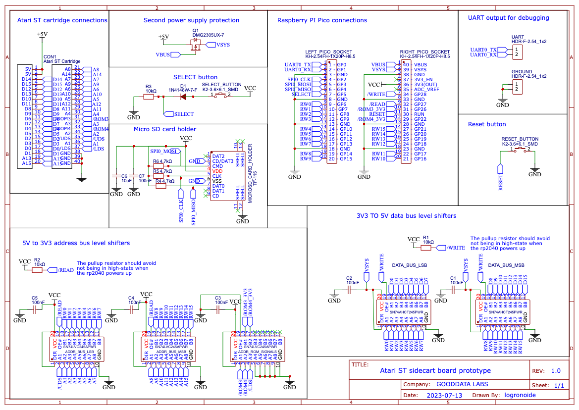
Within this schematic, the diverse hardware subsystems of the board are identified and sectioned accordingly. Below are detailed descriptions of each component:
5V to 3V3 Address Bus Level Shifters
The 5 to 3.3 volts and TTL to CMOS subsystem converts all cartridge port input signals to the appropriate voltage levels for the RP2040. This subsystem comprises the following components:
- 3 x SN74LVC245APWR: An 8-bit bus transceiver with 3-state outputs. The direction is set with the inputs as TTL and the outputs as CMOS. This component converts the address bus from 5V to 3.3V. The !ROM3 and !ROM4 signals are also converted from 5V to 3.3V with this component. The !LDS signal is ignored since it is not used on the SidecarT board. The !UDS signal is connected as the A0 input signal. The ADDR_ROM_SIGNALS are only working as a level shifter because the !OE (Output Enabled) signal is always enabled, but the ADDR_BUS_LSB and ADDR_BUS_MSB are taking advantage of the three-state output of the IC to set the output of the address bus to floating depending on the !OE signal connected to the !READ signal generated by our code in the RP2040. Therefore, the RP2040 can read from the address bus when the !READ signal is active and the address bus is floating when the !READ signal is inactive. The ADDR_BUS_LSB and ADDR_BUS_MSB are connected to the RP2040 GPIOs GP6 to GP21. The !ROM3 and !ROM4 signals are connected to the RP2040 GPIOs GP22 and GP26 respectively. The !READ and !WRITE signals are connected to the RP2040 GPIOs GP27 and GP28 respectively.
- A pull-up resistor connected to the !OE signal of the ADDR_BUS_LSB and ADDR_BUS_MSB ICs. This resistor is used to set the output of the address bus to floating when powering on the SidecarT board. Otherwise, the Atari ST could read garbage from the address bus that could lead to a crash.
3V3 to 5V Data Bus Level Shifters
The 3.3 to 5 volts and CMOS to TTL subsystem converts all RP2040 output signals to the appropriate voltage levels for the Atari ST. This subsystem is composed of:
- 2 x SN75AHCT245PWR: An 8-bit bus transceiver with 3-state outputs, with CMOS inputs and TTL outputs. This component is used to convert the data bus from 3.3V to 5V. The DATA_BUS_LSB and DATA_BUS_MSB are connected to the RP2040 GPIOs GP6 to GP21, sharing the same GPIOs with the address bus. The !WRITE signal is connected to the RP2040 GPIO GP28. The DATA_BUS_LSB and DATA_BUS_MSB take advantage of the IC’s three-state output to set the data bus output to floating, depending on the !OE signal connected to the !WRITE signal generated by our code in the RP2040. Thus, the RP2040 can write to the data bus when the !WRITE signal is active, and the data bus is floating when the !WRITE signal is inactive.
- A pull-up resistor connected to the !OE signal of the DATA_BUS_LSB and DATA_BUS_MSB ICs, functioning in the same way as the pull-up resistor of the address bus.
Reset Button
Remarkably, the Raspberry Pi Pico W lacks a reset button, an omission rectified on the SidecarT board.
UART Output for Debugging
For debugging purposes and directing output to the Raspberry Pi Pico W’s serial console debug traces, GP0 and GP1 are connected to the RP2040’s UART output.
Raspberry Pi Pico Connections
Additional details are available in the Hardware Interface section.
Second Power Supply Connection
The SidecarT board permits power sourcing from two distinct points: the Atari ST cartridge port and the Raspberry Pi Pico W USB port, offering voltage levels of 5V and optionally 3.3V (dependent on the USB port used). The diode DMG2305UX-7 ensures that power is sourced from the Atari ST cartridge port when available and defaults to the Raspberry Pi Pico W USB port otherwise, preventing simultaneous connection of both power sources.
SELECT Button
Connected to the GP5 GPIO of the RP2040, the SidecarT board’s SELECT button facilitates the selection of operational modes. To ensure the switch remains off upon powering on the SidecarT board, a pull-down resistor is linked to this GPIO. Additionally, a 1N4148W-7-F diode, while not imperative, is connected to this GPIO to safeguard the RP2040.
Micro SD Card Holder
The TF-115 model micro SD card holder is interfaced with the RP2040’s SPI0, with connections as follows:
- CLK: GP4
- MOSI: GP5
- MISO: GP6
Absence of a CS connection is due to the RP2040’s GPIO limitation. While the CS signal would typically connect to CD/DAT3, it is connected to GND as no additional slave devices are present on the SPI0 bus.
Pull-ups and capacitors are connected as detailed in the Hardware design with RP2040 datasheet.
Atari ST Cartridge Connections
Refer to the Hardware Interface section for further details.